JLCPCB : Monitor Solar Panels Production (Part 5)
I always wanted to print my own PCB. This is so cool to see his own design getting to life. There are a couple of online PCB makers and I'm ready to test one of them ! But how does it work ? What should I do ? How much does it cost ? Where to start ?!?
Fritzing
Let's rewind a little. In the first episode, we have created a schematic design, in this episode, we are going to create a physical design. I'm using Fritzing to create my original schematic design and based on that, the software can generate a breadboard view and a PCB view.
You can jump from one view to another using the tabs at the top of the screen :
The breadboard view is nice when it comes to start building the initial prototype. The generated view could be a little bit messy, you will have to rearrange the components.
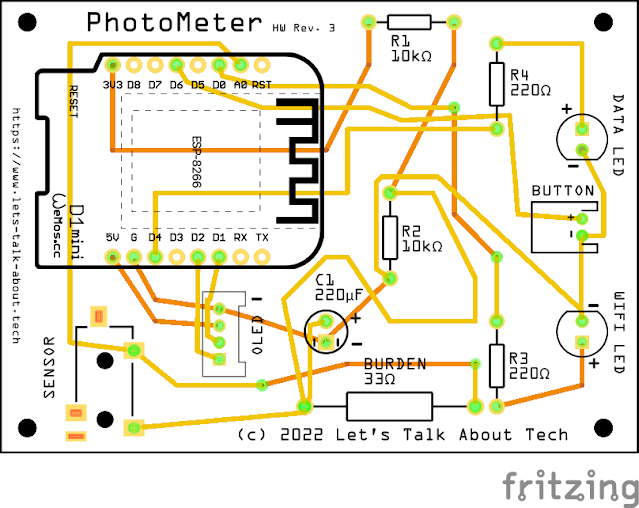
Switching to the PCB view now, this is the real circuit board as it will be created by the manufacturer. You have to understand this view is actually a 3D view with different layers. The top layer and the bottom layer. Why this ? Remember when creating the circuit with the breadboard, sometimes the wires and crossing each other. On the breadboard, it works because each wire got insulation around the conductor. On the PCB, this is not the case anymore, conductors are exposed therefore, "wires" cannot cross each other without create a short circuit.
This is why PCB makers invented the "Vias". These are little holes sending the connectivity track to the other side of the board to avoid crossing another conductor. On the below circuit, lines in yellow are on the top side and lines in orange are the bottom side.
In simple PCB design for DIY like here, we can manage two layers. Some Intel PCBs can go up to 6 layers ! The reason ? to have circuits as small as possible to reduce the form factor as well as optimizing circuit for speed and performance.
When you are happy with your design and when all routing rules are satisfactory, you can export your PCB design as a GERBER file.
GERBER files are a list of instructions the PCB factory requires to actually make the PCB following your specifications : Layout, size, position, holes, text, .... When you have exported the required files (all together in a ZIP), you will have to find an Online PCB maker.
It exists a couple on the Internet, most if not all, located in China.
JLCPCB
I have decided to give a try at JLCPCB. I've seen a factory tour few month ago and I was quite impressed by the process. Many youtubers that I'm following in the DIY/electronic game are using JLCPCB and the quality of their builds seem very impressive !
The company has been founded in 2006 and employs more than 3000 employees. Here are some company facts :
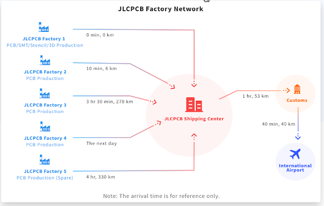
So, JLCPCB is actually composed of 5 factories and a shipping center. From there, they are able to control the entire chain. Cleverly situated close to the customs and airport to be efficient on the deliveries.
JLCPCB developed a full digital experience, from the order to the delivery, you can follow every aspects of the manufacturing from keyboard to your mailbox. This is very impressive and I actually never seen something like this.
Let's build it
Let's send the GERBER zip file and see how it goes. It is an easy process, you just have to drag and drop the ZIP file on the website home page and automatically, the process is starting.
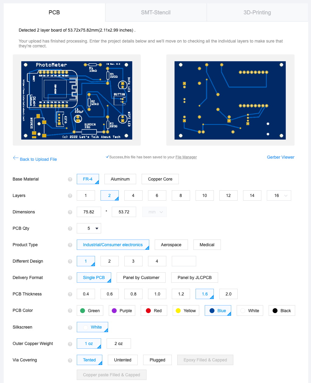
You have the ability to see the PCB in 3D to control if everything seems right, you can chose the color of the PCB, the color of the stencil, ... and tweak some parameters. Of course, check the pricing on the side, it is updated in real time.
If speed is a concern, some parameters are more time consuming, so choose them wisely. For example a green PCB is faster than any other color. Reason is : most customers are using green, if you choose blue for example, they are waiting for more blue orders to combine them together on the same blue PCB plate.
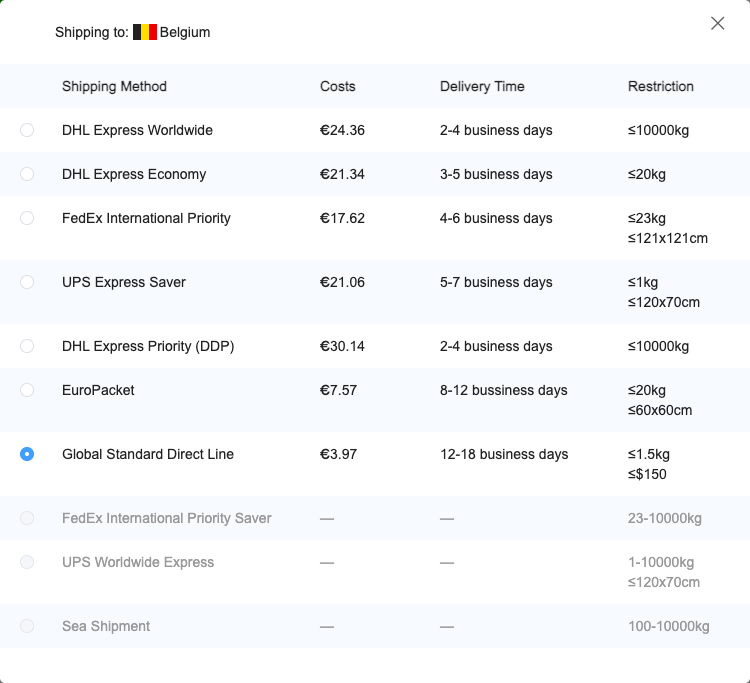
To optimize the cost, you can choose between different carrier for the shipment. From Standard China Post to Fedex or DHL. Depending how keen you are to get your order ;) I have tested the cheapest with tracking and Fedex - I'm based in Europe. The difference is not impressive. 14 days for the cheapest tracked against 8 days for FedEx.
Here are the various options :
Manufacturing process
Ok you have configured all your options and your shipping carrier, your payment is done, but what's next ?
There are 3 majors steps before your receive your order :
- Your design is verified by a JLCPCB engineer
- The manufacturing process starts
- Your order is shipped
You know the feeling, when we order something we always check what's going on, where is my order, how long will it takes before shipping ....
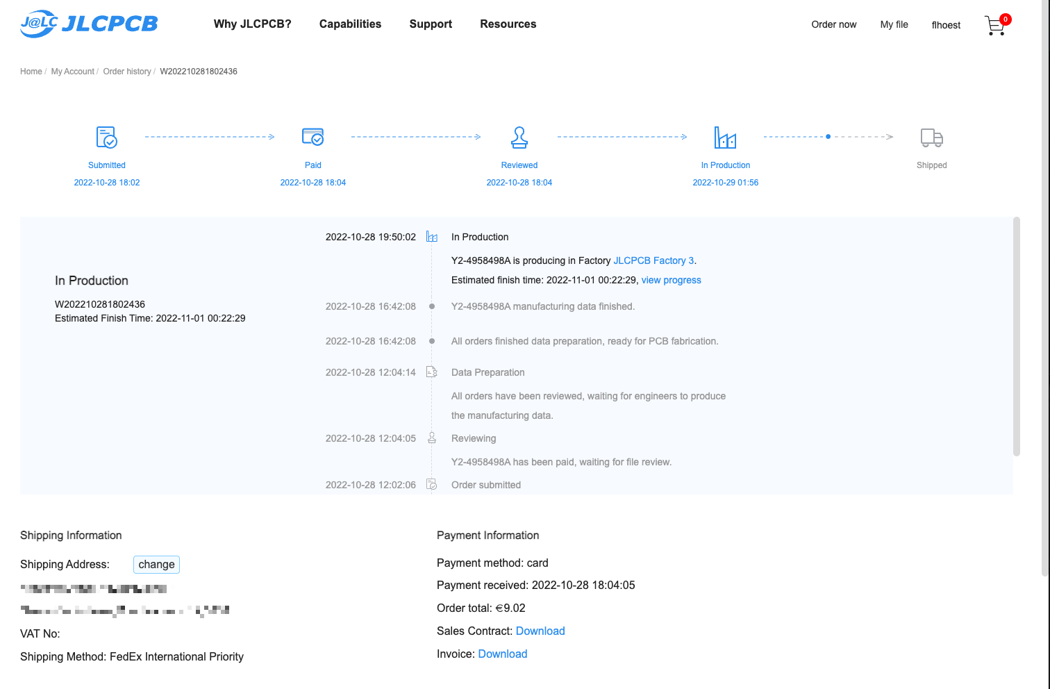
With JLCPCB, this is amazing, you have answer to all these questions ! You can check the status of the manufacturing process in real time. I really wonder how they can achieve that.
So first, you know in what factory your order is made. You can then see how far from customs and airport you part is. My below order is from Factory 3 ;)
Not only you have the estimate time for finishing your part, but as well all the differents steps are clearly explained and you known when each steps have been completed. Honestly, this is an example for many other online shops. I'm really amazed. I'm doing online shopping since 1997 and I never seen something similar.
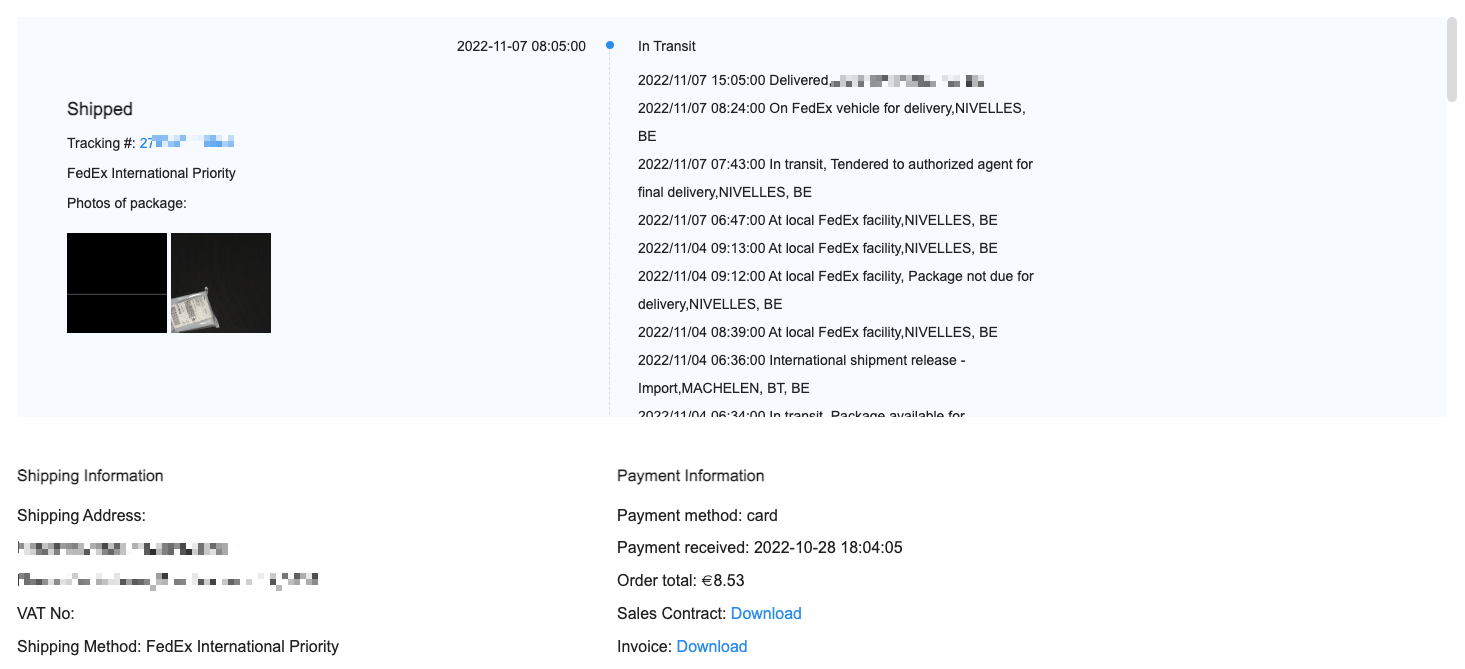
But wait, there is more. You even got the courier tracking in the JLCPCB website as well as pictures from your order !
This is what you get :
Minimum quantity on each order is 5, so you can either try whatever you want when assembling or create multiple objects.
I definitely recommend JLCPCB for the quality of the finished product as well as the online shopping experience.
Let's heat up the soldering iron !
The fun part is soldering all the components. The rule is simple, always start with the smallest part and you should be fine. When done, I plugged the WeMos Mini on top of the hat and voila !
Here is PhotoMeter v3 !
This is neat ! For a first attempt, I'm very happy with the final result. Now, this is time to integrate all this in my enclosure ! The only difference between my GERBER files and the final result is the batch number JLCPCB added on the PCB. This is an internal reference they use to track their PCB I believe. There is an option when ordering the part to remove it. It has a cost, you can do it if you want. Honestly, I don't mind having this reference on my printed parts. If I was a reseller of electronic products it would probably be different...
Don't hesitate to generate GERBER files and print them with JLCPCB, this is not very expansive and this is really bringing your projects to the next level !
I hope this helps you to remove the fear of the GERBER files....
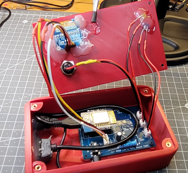
Here is the PCB in our own enclosure :
This is so cool ! I can now create more like this and even faster. The finish quality is top ;)
If you have made this project, please comment and let me know what you think about it ! ;)
What's next ?
Well, at this stage we did a lot of progress and we are close to something really professional. In its current state, is the product sellable ?
I think, not just yet.
We need :
- Debug the code and test is with a strong test protocol
- The case of a Internet/WiFi outage while running should be addressed :
- keep the data in a buffer, when Internet is back, push the data;
- If WiFi drops, try to reconnect
- Create a setup guide and procedure;
- Create product name, product image;
- Create packaging;
- Find a manufacture able to mass produce it








Comments
Post a Comment
Thank you for your message, it has been sent to the moderator for review...